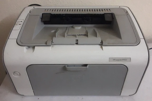
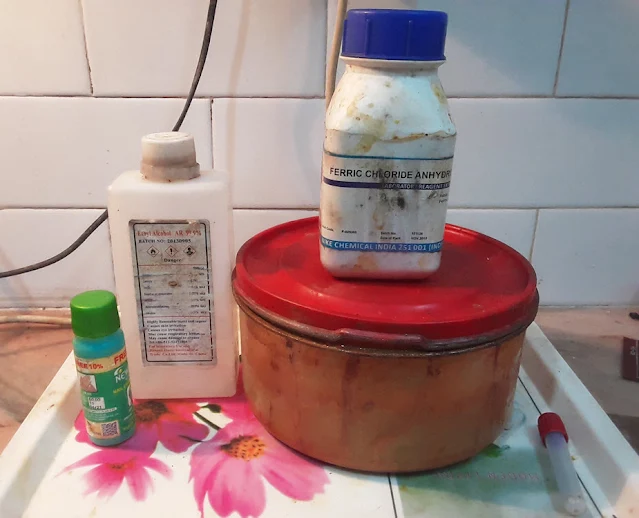
Here PCB design process of a custom breakout board for the L298N is illustrated. The PCB design steps are explained. This PCB design can be useful for small to moderate large PCB design. Making custom printed circuit board at home is helpful because for testing and prototyping it is quicker to do this at home rather than using PCB manufacturing service as it can take time for the PCB to arrive from PCB factory. So here custom PCB design and circuit board assembly using Proteus Professional PCB design software.is illustrated.
To follow this PCB custom design the following materials are required.
1. PCB design software(Proteus used here)
2. L298N IC
3. 15 position Header connector
4. Photopaper
5. Inkjet printer
6. Chemicals
a. Noil Polish Remover
b. Ferric Chloride(container for water+ferric chloride)
c. Ethyl Alcohol
d. Mixing tube
7. PCB copper board
8. PCB drill hole machine
9. Soldering Iron + Solder Wire
The steps to make custom printed circuit board at home is as follows.
1. Design Circuit schematic
In Proteus we can design the PCB layout easily. First we have to make a schematic capture of the what component we want to do the PCB design for. Here we need the L298N component and it's footprint for the 15 leads multiwatt package which is available by default in proteus. Then we need a header pins with 15 position and 1inch or 2.54mm spacing between the pins. The schematic capture and connection is shown below.
2. PCB layout and printing
Once the component are connected we can proceed to the PCB design part. The following is the completed PCB layout for the breakout board.
Optionally, proteus also provides 3D view of the designed electronics parts so that we can have a look how the final designed system looks like and check for any error. The 3D view of the breakout board is shown below.
The following video illustrates the PCB layout design process in Proteus.
3. Printing PCB layout on Photopaper
Once the PCB layout is completed the next step is to print the PCB layout. As shown in the above video, one the PCB layout is adjusted for printing, it is printed on a photopaper shown below. The printer type that should be used is Inkjet Printer.
4. Cutting PCB
The next step is to cut a PCB from a larger PCB clad. The size of the PCB to be cut is the size of the PCB layout on the photopaper. The cut PCB should be thoroughly washed to remove any dirts. Metallic scrub can be used to make the PCB surface a bit rough so that later on the PCB ink gets more easily attached to the PCB copper board. After washing the cut PCB the PCB is cleaned using the ethyl alcohol to remove any oil particles on the PCB.
5. Imprint PCB layout Ink onto PCB
The next step in making custom printed circuit board is to imprint the PCB layout ink onto the PCB copper board. This is the most crucial part for good custom PCB production. Here we take 50% ethyl alcohol and 50% nail polish remover in a small tube and mix them thoroughly by shaking the tube. The liquid mixture is gently spread on the PCB. Then the photopaper PCB print is placed at the top of the PCB. The PCB photopaper print is allowed to rest on the top for 1mins or less. Then the photopaper print and the PCB copper board are pressed hard together so that the ink is imprinted on the board. The mixture created earlier can be poured during the pressing process to obtain better imprint result. The photopaper will stick together with the PCB board and this is then put into water for over 4 mins. After that it is taken out of water and the photopaper is gently and slowly removed from the board. Then you should see the ink trace remaining on the board as shown below.
6. Etching off Copper
Next the PCB imprinted with the ink trace is dissolved into the ferric chloride plus water solution to etch off the copper except the copper underneath the ink trace.
The PCB board in the solution is stirred and/or the container is shaken so that the chemical reaction is quicker to help the copper removal quicker. After a while the PCB board is taken out and the board should contain only copper traces as shown below.
7. Removal of PCB ink
Next, we remove the PCB ink from the board using ethyl alcohol. Here we can use toothbrush or similar brush to help in the removal process. After the PCB ink is remove the PCB board looks like the following.
8. PCB board drill
The next step is to drill the holes in the PCB. For this PCB drill machine with appropriate drill bit is required. An expensive drill machine like the following can be used.
9.Circuit board assembly
The final step is to populate the components L982N and the header onto the drilled PCB board. For this a soldering iron and solder wire are required. The final completed L298N breakout board is shown below.
So in this way Custom PCB design for L298N breakout board can be made. The breakout board is designed to fit on the breadboard for easier circuit testing and prototyping. This breakout board usage is illustrated in the tutorial DC motor speed control with Arduino PWM and Potentiometer.
Below are some application of L298N motor driver.
- How to use L298N motor driver with Arduino
- Arduino L298N DC Motor Speed control with PWM
- Speed and direction control of DC motor using Arduino Fast PWM


